Main menu
You are here
Power Theory: The Distribution Network
Introduction
After completing my research on real devices, I was ready to tackle power systems. I chose to start at the top and work my way down to the details. This article discusses power systems from a top level view and then explains how to design a power distribution network. We don't consider power system design, feedback or control here. The focus will be on the power distribution network. Almost everything I talk about here I learned from my colleagues.
Power System Overview
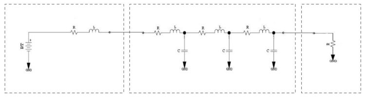
When you think of power, the lay person tends to think of some source of power (a power plant) and the object that consumes that power (the air conditioner in their house). What is overlooked is how the power from the source gets to the load. This is the distribution network. This can be anything from giant power lines to the trace that connects the power pin of an ASIC to a power plane.
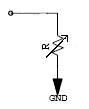
Loads
Loads in a system are typically modelled as variable resistors. A load which increases its current draw is really lowering its impedance.
Resistors aren't completely accurate models of loads. Loads have an impedance plot like any device and will have varying impedance over frequency. This plot will also change over time as its current consumption varies over its range of functions. This, however is relatively unimportant for a couple of reasons. First, as long as you know the maximum frequency at which the load will switch you can simplify your design by focusing on that worst case scenario. Second, as long as you know the maximum ripple you can design your distribution system to never display a ripple higher than the maximum at the worst case frequency and below (to ƒ=0).
Keep in mind that modern devices with low voltage rails consume large amounts of current (10's of amps) and have extremely high di/dt (1000A/μs). This is due, I think, to the large amount of transistors switching inside the ASICs. As a result, it's important to consider the steady-state maximum current draw and its transient current draw as well.
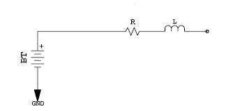
Power Sources
For our sake, power supplies can be modelled as an ideal power source in series with a resistor (R) and an inductor (L). The resistor is the steady-state impedance of the supply. The inductor is an intrinsic property of power supplies and can be responsible for spikes seen during sudden changes in load. A capacitor (C) could also be placed in parallel with the ideal power source which helps model the ramp up during first power on.
| R=VOUT/IMAX |
 |
Power supplies are often slow devices, only capable of delivering di/dt in the thousands or 10's of thousands. This must be taken into consideration when designing a distribution network because it will be required to not just transport energy, but to store it as well. It must be stored in such a way that extremely fast delivery will be possible.
Distribution Systems
As previously discussed, a distribution must accomplish several things simultaneously:
- Deliver power from the source to the load efficiently.
- Compensate for the slow "speed" of power supplies by supplying fast energy.
- Eliminate noise (ripple) where possible.
The model is fairly simple. An unloaded distribution system is composed of a small amount of resistance and inductance in series. A loaded, or decoupled system breaks this resistance up into chunks by placing capacitors at certain spots in the network (e.g. at different points along the length of a trace).
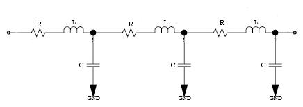
Design
The design is broken down into six steps: 1) selecting your target impedance, 2) determining your target ƒmax, 3) selecting a set of capacitors, 4) geographical placement of the capacitors, 5) determining the power efficiency and 6) selecting the amount of capacitors you will be using.
Step 1: Select Target Impedance
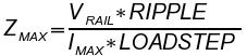
The amount of acceptable ripple will depend on your design. The ripple is caused by the inductance present in the distribution network and the di/dt of the load. The touchiest ASICs usually require ±5%. Most distribution networks try to achieve a ripple of <2%. With this value you can calculate the maximum impedance your distribution network is allowed. Using Ohm's Law we calculate the impedance knowing that the maximum voltage is the total allowable ripple and the maximum current step to cause this ripple (think in terms of V=L*di/dt) is the load step current. We will consider the voltage drop caused by resistance later. The load step in modern power design is 50% (in other words the circuit always draws approximately half the total current).
| Zmax=(VRAIL*RIPPLE%)/(IMAX*LOADSTEP%) |
 |
Step 2: Determine ƒmax
Your maximum frequency is determined by the loads. ASICs need 100-200MHz. This is a design challenge as we'll see when we analyze geographical placement.
Step 3: Develop Capacitor Models
Depending on your resources, you are going to need some information on the caps you wish to use. It's a good idea to get models from the vendor or if you have the expertise do your own testing in a lab. You can get away with using the ESR and ESL of the caps without too much trouble. Once you have a set of caps ranging from small (high frequency) to large (low frequency) we can begin designing our distribution system.
It's worth mentioning here that the PCB is another source of capacitance and must be considered as a separate component. It's also worth noting that the power supply is an inductor and must be taken in to consideration as well.
One note on speed: The speed of a capacitor is typically much faster than a power supply. Switching power supplies can't react to really fast changes in the load. As a result the RC time constant of a capacitor and the load (especially the small ones very close) is typically very small and is capable of responding (providing energy) to the very high di/dt seen in ASICs.
Step 4: Determining Geographical Requirements
We know that at a high enough frequency, inductive reactance will dominate capacitive reactance. This is especially true at high frequencies with large caps. At a certain point the inductance of the traces, ASIC pins and vias (yes!) will overpower the capacitor. Therefore, you must be careful in where you place your capacitors. The common approach is to determine the maximum distance that a capacitor is effective and call that the radius of a circle. You know that where you place that cap, it will provide effective decoupling.
This can be done one of two ways, graphically or with equations. Plot the impedance of your trace at say, 3" (this includes capacitor and mounting inductance as well as trace inductance), against your graph of capacitors (you did make a graph, didn't you?). Any caps on the left of the trace plot are ineffective at that distance. The ones to the right will still be capacitive.
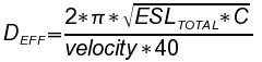
Using equations, you can determine the effective radius of a capacitor using the total ESL and the velocity of the board material.
| DEFF=(2*π*sqrt(ESLTOTAL*C))/(velocity*40) |
 |
Calculate the radius for all your caps. It may be easier to bunch caps into groups to make CAD more reasonable.
Step 5: Minimum Power Efficiency
We have calculated the transient voltage drop, but what about the steady-state offset? This is typically compensated for by the power supply design using feedback. This way the voltage rail stays at the proper value. However, this means the system has to constantly compensate for this undervoltage condition. This undervoltage translates to power loss and lowers the efficiency of the distribution system. The efficiency of the system is usually 98-99% and is fairly easy to achieve.
The maximum voltage drop is calculated using a maximum load condition.
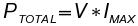
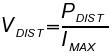
| PTOTAL=V*IMAX | PDIST=PTOTAL*(1-eff%) | VDIST=PDIST/IMAX |
 |
 |
 |
When we finish the design, we can calculate this value to insure that all our capacitors combined does not exceed this value. Remove the load and source from the circuit. Then replace the inductors with shorts. Now replace the capacitors with their ESR. Calculate this resistance value and you will have a decent approximation of the distribution resistance.
We can now begin the design of our power distribution network.
Step 6: Design The Network
Now that we have our requirements set straight, we can design our network. This is best done in a spreadsheet or in spice. The easiest way is to select a set of caps across the range and plot the impedance over frequency. This result will tell you where your holes are (i.e. too much impedance). Once you've got a nice flat line, it's time to look at the geography. Often times this minimum capacitance won't be enough. You'll have to add more caps of the same value to provide coverage over the entire board. Basically, if a cap provides 4 square inches of coverage and your board is 16 square inches, you'll have to quadruple the number of caps. This is not a problem, it will just decrease the impedance of the board. It does raise cost, probably a few dollars/board.
It would be a good idea at this point to calculate the power efficiency of your board. The leakage of the caps will eat up your power budget and more caps add up.
Now that you have your decoupling taken care of, what's remaining is the actual work: schematic capture and layout. Be sure to keep your caps spread out over the board.
Most power supplies have a ramp up feature which provide protection against in-rush. So, in-rush is not much of a worry.
Illustrative Design Example
This example will illustrate the principles I've laid out in this article. The numbers I've chosen are a bit cooked up, I admit, but they are not too far fetched. The only thing that may not be realistic for some designs is that I've made the power requirements small so the amount of decoupling capacitors I need will be too.
Our example will be a 5" by 10" PCB with a power supply delivering 12V@10A for a total of 120W. It has been decided that 5% ripple, a 5% distribution loss and a maximum switching frequency of 100MHz will all be acceptable. The load step will be 5A (or in other words the minimum load is always 5A and the maximum load will be 10A, so 10A-5A=5A). The board material is FR-4 and that gives us a velocity of 180ps. Mounting inductance is the same for all devices at .3nH. The capacitance for a 5" by 10" board (simplified to a simple two layer cap) is 20nF.
To summarize:
- PCB: 5" x 10"
- PS: 12V@10A
- Max Ripple: 5%
- Max Distribution Loss: 5%
- Max Switching Frequency: 100MHz
- Load Step: 50%; Load Step Current: 5A
- Board Material: FR-4; Velocity: 180ps
- Mounting Inductance: .3nH
- PCB Capacitance: 20nF
Step 1: Select Target Impedance
ZMAX=(12V*.05)/(10*.5)=0.120 ohm
Step 2: Determine ƒmax
This was previously determined to be 100MHz
Step 3: Develop Capacitor Models
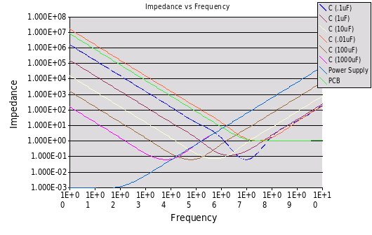
Capacitors were modelled using an R-L-C circuit for .01uF, .1uF, 1uF, 10uF, 100uF and 1000uF. The PCB and power supply are also modelled. The actual values used for all the components are listed below.
| Device | Resistance | Capacitance | Inductance | L+Mounting L |
| .01μF | .01 | .01μF | .01nH | 3.01nH |
| .1μF | .05 | .1μF | .1nH | 3.1nH |
| 1μF | .05 | 1μF | 1nH | 4nH |
| 10μF | .05 | 10μF | 10nH | 1.3nH |
| 100μF | .05 | 100μF | 100nH | 1.03nH |
| 1000μF | .05 | 1000μF | 1000nH | 1.003nH |
| Power Supply | .001 | 0.0 | 1μH | N/A |
| PCB | 2.0 | 20nF | .01nH | N/A |
Their impedance plot is as such:
Step 4: Determining Geographical Requirements
Mounting inductance is .3nH. Calculating the the distance gives the following results:
| Capacitor | Effective Radius |
| .01μF | 1.54" |
| .1μF | 5.52" |
| 1μF | 31.5" |
| 10μF | 280" |
| 100μF | 2760" |
| 1000μF | 27600" |
Step 5: Minimum Power Efficiency
This design only requires a power efficiency of 95%.
PTOTAL=12V*10A=120W
PDIST=120@*(1-.95)=6W
VDIST=6W/10A=.6V
We will come back and recalculate the efficiency values after we pick the type and number of caps for our design.
Step 6: Design The Network
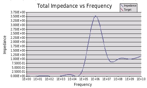
Here is what the PCB with the power supply looks like with no decoupling. As you can see the power supply is a problem after 100kHz. The board capacitance helps reduce the inductance at very high frequencies, but there is a very high peak at 1MHz. 3.5 ohm at 5A could cause a large voltage drop, not to mention a 5V drop in the power supply due to inductance. The short answer is this would not work!
Here is the graph after adding a few components. You can see how it has flattened down and meets or beats our target impedance.
| Capacitor | Number |
| .01μF | 10 |
| .1μF | 1 |
| 1μF | 1 |
| 10μF | 1 |
| 100μF | 0 |
| 1000μF | 0 |
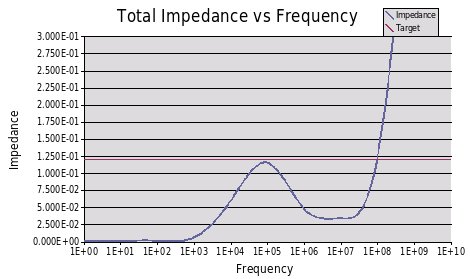
Now the caps selected all have a radius larger than the size of the board except the .01μF. This requires a muliplier of 7 bringing the total caps on the board to 73. The smaller caps should be placed close to the ASIC and other loads.
Calculating the power loss of the decoupling caps (I took a short cut by calculating several resistors in parallel), I got a resistance of .05/73=.685 μohm. At 10A this is a 7mV drop across the distribution which is well within tolerance.
Analysis
Now that we have designed the system, we should analyze it to understand how it works. For the sake of brevity I will analyze 1 capacitor at 1 particular frequency, otherwise it would be too cumbersome to calculate by hand.
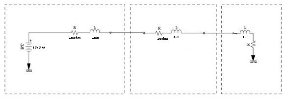
This is the system with no decoupling caps. Notice how large the spike is with a di/dt of 1A/μs compared to steady-state losses!
di/dt=1A/μs
I=4A
VPS_LOSS=4A*1mohm=4mV
VDIST=4A*2μohm=8μV
VTRANS=L*di/dt=7V
This could damage or at least disrupt the functionality of the chip.
Now we add one decoupling cap to the circuit.
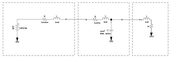
First we analyze the loop with the capacitor and the load.
di/dt=1A/μs
VL1_TRANS=L*di/dt=1μH*1A/μs=1V
1V is still pretty high, almost 10%. If we placed the cap closer we could reduce the inductance (the packaging inductance of the ASIC is <<1μH). Now to calculate the di/dt for the loop with the cap and the power supply. The voltage across the cap should discharge and cause a current to flow through the cap. Here the cap supplies the power to the ASIC. If this were a lone capacitor it would eventually discharge to 0V, but it has a power supply behind it and in reality will never fall very low so the 0.1 is a fudge factor and is probably high (12-11.9=0.1). This circuit should really be analyzed in spice so our numbers are very rough.
dV=(0.1)(1-1/e1μs/.4*10μF)=22.1mV
I=C*dv/dt=10μF*22.2mV/μs=221mA
di=(0-221mA)(1-1/e1μs/.4*10μF)=-48.9mA
VL2_TRANS=L*di/dt=6μH*-48.9mA/μs=-294mV
What we see in the power supply loop is a much lower voltage and a lower current. This will charge the cap over a longer period of time. This is a great result because our power supply is not stressed and is not required to act faster than it can.
References
Personal Correspondence
Papers by Larry Smith (Sun Microsystems)
High Speed Board Design Advisor, Power Distribution Network from Alterra Corporation
Add new comment